
Tesla Traction Inverter Gate Drive Deep Dive
Tesla traction inverters have always been particularly interesting to me because the power stage is constructed from paralleled discrete devices instead of a single large power module. This philosophy is shared with their battery packs, which were originally thousands of 18650 cells. Most other car companies like to buy either three phase-legs or a single sixpack power module to build their inverter, and a smaller quantity of large format prismatic cells to build their battery pack. There are certainly technical merits to each approach, but I would argue the main difference is how much of the engineering work you would like to offload to your suppliers.
Model S/X Small Drive Unit Inverter
Let’s take a look at the small drive unit inverter from the Model S and Model X dual motor vehicles. This one comes from a 2015 Model S 70D that was in a flood. Water did get inside the inverter through the access port on the drive unit used to bolt the three phase cables to the motor windings, but after some cleaning, it is still functional thanks to the conformal coating and silicone potting.

The exploded view looks something approximately like this:
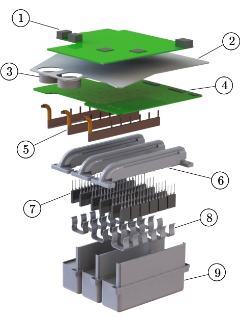
- Control board
- Aluminium shield
- Phase current sensor ferromagnetic core for MLX91209 hall effect sensor
- Gate drive board
- Phase busbars
- Heat sinks
- TO-247 package IGBTs
- IGBT clips
- DC-link film capacitors (Panasonic 450uF/430V).
The DC+ and DC- busbars are not shown, they are directly under the gate drive board. The Y-capacitors are also not shown, they are packaged near the DC input connector.
Paralleled Discrete IGBTs
Each of the six switches are formed by six paralleled International Rectifier (IR) AUIRGPS4070D0 IGBTs. These are likely binned by Vce,sat to ensure good current sharing when paralleled. The datasheet claims 240A continuous collector current, however later states the continuous current is actually limited to 195A by the package. Either way that results in potentially somewhere around 1000Arms of phase current capability, at least for a short time. At full modulation index with a 400Vdc bus, that is about 490kVA of peak power.
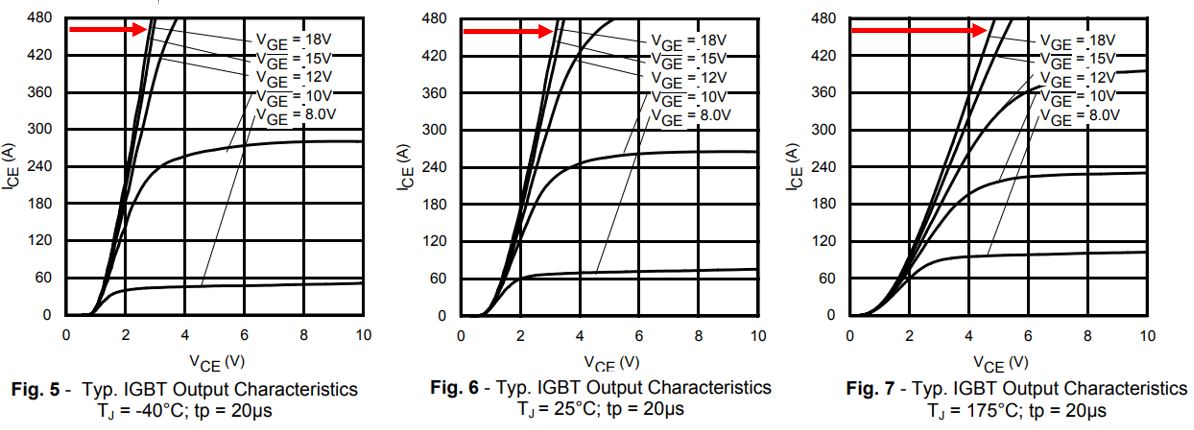
From the output characteristic curve variation over temperature, it is clear the device has a positive Vce,sat temperature coefficient. This will help with the static current sharing, as any device conducting more current will get hotter, increasing its Vce,sat, which will reduce how much current it is conducting, naturally balancing the parallel device currents. Putting all paralleled devices on the same heatsink will also help limit any case temperature variation that could lead to deviations in Vce,sat.
Gate Drive
The dynamic current sharing is influenced significantly by the gate drive layout. The gate-emitter loop impedance between the driver and each device must be closely matched, as it determines what the gate of each device sees during a switching transition. Since there are not too many examples out there of how to do this layout properly, I thought it would be interesting to investigate the gate drive board in more detail. Please ignore the silicone potting material on the PCB, it’s a huge pain to remove and I haven’t found a solvent that helps.
Isolated Supplies
First let’s take a look at how the isolated +15/-8V rails are generated, shown in yellow in the top left. There are four isolated supplies, one for each phase’s highside switch, and a common lowside (since all the lowside IGBT emitters are referenced to DC-). On the back side of the board there is a transformer marked TDK 222S6A12. The same one is used in the Model 3/Y inverter. The TDK catalog only has a 200S6A12, but I would guess the 222 version is the same part with a slightly different turn ratio, as 0.7 / 1.2 doesn’t quite give the 8V/15V rails needed. The part is specifically recommended for inverter applications, and since they are using it with SiC FETs in the Model 3/Y, it must have a low leakage capacitance to deal with the large dv/dt on the secondaries.
![]()
The primary side drive is accomplished with the TI UCC2803 current mode controller driving an IR AUIRFR3806 60V/43A FET off the main 12V rail. Feedback across the gap is done with a Broadcom M49T opto.
Driver ICs
The gate drive ICs are Infineon 1ED020I12FA2 single channel drivers. These include desat detection and active miller clamping, however the active clamp is unused as the bipolar (-8V) supply makes it unnecessary. These drivers are rated for 2A rail to rail output. A quick look at the IGBT datasheet shows a typical total gate charge of 250nC and rise time of 125ns. Multiplying the gate charge by 6 IGBTs and dividing by the rise time gives a rough estimate of 12A of gate current. Evidently the gate driver output will need to be further amplified.
Driver Amplifiers
To supply the required gate current, the driver output is fed to second stage of FETs. I took some time to trace out the circuit, as it is not as simple as I would have thought, and arrived at the schematic below. In the schematic, Vdriver is the output of the gate driver IC which swings between -8 and +15V. Zener diodes are used to bias the gates of the FETs. I measured the zener breakdown voltage to be somewhere around 10V. The main drive FETs, M3 and M4, are Infineon OptiMOS power FETs, IPD50N04S3 and IPD50P04P4L respectively.
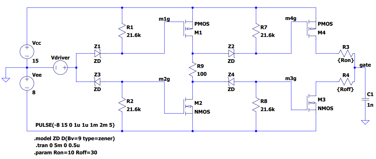
When the driver is in the off state, outputting -8V, the voltage across Z1 exceeds the zener voltage, due to the pullup R1, and the zener begins reverse conducting bringing the gate of M1 down to -8+Vz, or about 2V. This turns on M1, since it is PMOS, bringing its drain up to Vcc. Z2 has no voltage across it and is not conducting, so the gate of M4 remains pulled up to Vcc and M4 remains off. Considering the NMOS side now, Z3, like Z2 has no voltage across it, keeping the gate of M2 pulled down to Vee by R2, leaving M2 off. However since M1 is on, Z4 will now have approximately 23V across it because it is connected to the drain of M1 through R9. Z4 will begin reverse conducting, bringing the gate of M3 up to 15V-Vz, or about 5V. Since the source of M3 is -8V, Vgs will be well above Vth and the FET fully turned on.
Conversely (and a bit more concisely) when the driver is in the on state, outputting +15V, Z3 begins reverse conducting, turning on M2, which causes Z2 to start reverse conducting through R9, pulling the gate of M4 to approximately -8V+Vz, or 2V, fully turning on M4.
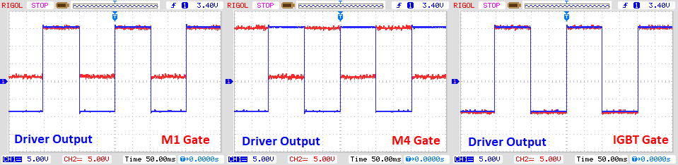
To check my LTSpice sim, I powered up the gate drive board and fed one of the phases some low frequency PWM. The scope output shows how the PMOS gate voltages are clamped to Vee+Vz and how the gate signal is inverted twice by the PMOS/NMOS combination, resulting in the IGBT gate being in phase with the driver.
Driver Layout
Here is how the layout is done. The highside FET M4 drain is directly connected to a wide trace on the top-side of the board which runs along the line of IGBTs, connecting to each gate with an individual 10 ohm turn-on gate resistor. The lowside FET M3 drain drops down to the bottom side of the board which has a similar trace and 30.1 ohm turn-off gate resistors.
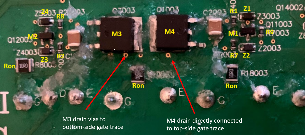
Note: I didn’t unsolder the board to check the turn-off resistors on the bottom, but measuring from one gate to another gate gives 15.1 ohms. Solving 15.1 = 1/(1/20 + 1/(2Roff)) gives Roff=30.1. Measuring the resistance between the drain of M3 and M4 gives 6.7 ohms, which is approximately 10/6 + 30.1/6, so it seems correct. I thought this was fairly large for a gate resistor, but I think you can consider that the “effective” gate resistance is really 5 ohms if the 6 IGBTs were paralleled internally, like they would be in a power module.
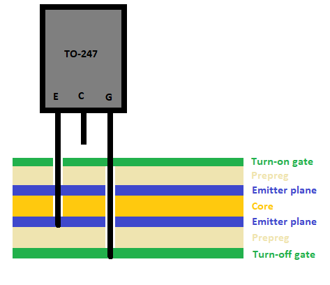
To minimize the loop inductance, for each phase, one or two internal planes of the four layer stackup are connected to the IGBT emitters. These are tied to the 0V point of the isolated supplies but also to the large ceramic capacitors adjacent to M3 and M4. The turn-on and turn-off traces on the top and bottom of the board run directly over the emitter planes, so the only resulting gate-emitter loop area is caused by the thickness of the PCB substrate. The best look at the internal planes I can get is from shining a flashlight through the backside of the board, but this is my guess for the stackup.
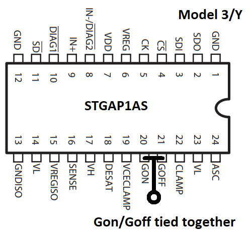
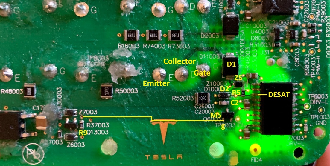
Interestingly, the Model 3/Y inverter uses a very similar setup:
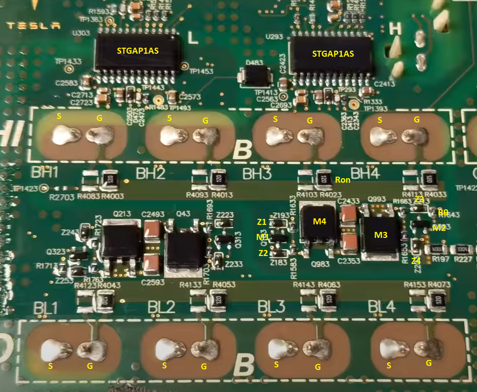
The Infineon drivers have been replaced with ones from ST, to match the ST SiC FETs, but the gate drive amplifier is essentially exactly the same, zener diodes and all. Unlike the 1ED020I12FA2, the STGAP1AS driver has separate turn-on and turn-off gate source/sink pins. Since the turn-on and turn-off discrimination is done externally by the amplifier stage, you can see the pins have been tied together on the PCB.
Desaturation Detection
The desat detection circuit is fairly standard, with an interesting twist. I added it to my original gate drive schematic, as the twist is that the desat circuit ties in to the gate drive amplifier.
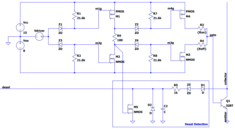
The general goal of desaturation detection is to determine when the IGBT is in a short circuit condition and turn it off before it blows up. To do this, the driver monitors the collector emitter voltage with the desat pin, and turns off the gate if the desat pin rises over a threshold (9V for the 1ED020I12FA2). The collector is not directly connected to the desat pin. Inside the driver, there is a 500uA current source charging the capacitor C2 through the desat pin. The desat pin voltage is therefore related to the collector emitter voltage as Vdesat = Vce+0.5mA*R5+Vz+Vf where Vz is the zener voltage of Z5, and Vf is the forward voltage drop of D1. If Vce rises above 9V-0.5mA*R5-Vf-Vz the driver will shut off the gate. Usually just D1 is used, but adding Z5 will cause the desat protection to trigger at a lower saturation voltage, controllable by Vz.
What is interesting is that the drain of M5 is also tied to the desat pin. M5’s gate is connected to the inverted stage of the amplifier circuit, such that M5 will turn on when the driver output is in the off state. The desat pin is then pulled to ground, effectively disabling the desaturation detection. Of course when the IGBT is already off, there is no need for desaturation detection and Vce is expected to be very large, so the gate drive IC should implement this functionality internally. The only theory I can come up with is that this is a work around for some spurious triggering of the desat pin during large dv/dt swings which cause current to charge the blanking capacitor through the parasitic capacitance of D1. In theory M5 will disable the desat pin relatively instantaneously before the IGBT switching transient actually occurs.
For some reason all the collector pins are marked “D” on the silkscreen instead of “C”.
Conclusions
Hopefully that sheds some light on how Tesla implements their paralleled discrete gate drive. The concept seems essentially unchanged in the Model 3/Y, with four 250A ST SiC FETs in parallel per switch, instead of 6 IGBTs, and an identical gate drive amplifier. If I got anything wrong or missed anything, please send me an email and let me know: john@ohm.ninja.