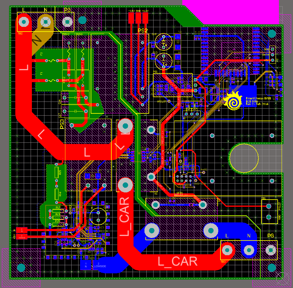
Internet Connected J1772 EVSE Design
Here’s a preview of the PCB layout I completed for an internet connected electric vehicle charger design. Since the design requirement was only AC Level 1 (15A/120VAC) the main current paths were done on the PCB itself with 2oz copper outer layers. This simplified the high voltage front end design which monitors voltage and current in real time. The board is four layers, mostly for EMI mitigation reasons. The internal layers allow for ground planes between the SMPS modules as well as the AC line voltage keeping most of the noise out of the ADC readings. The high voltage and low voltage sides of the board are fully isolated and I2C communication is done over the gap with the TI ISO1541.
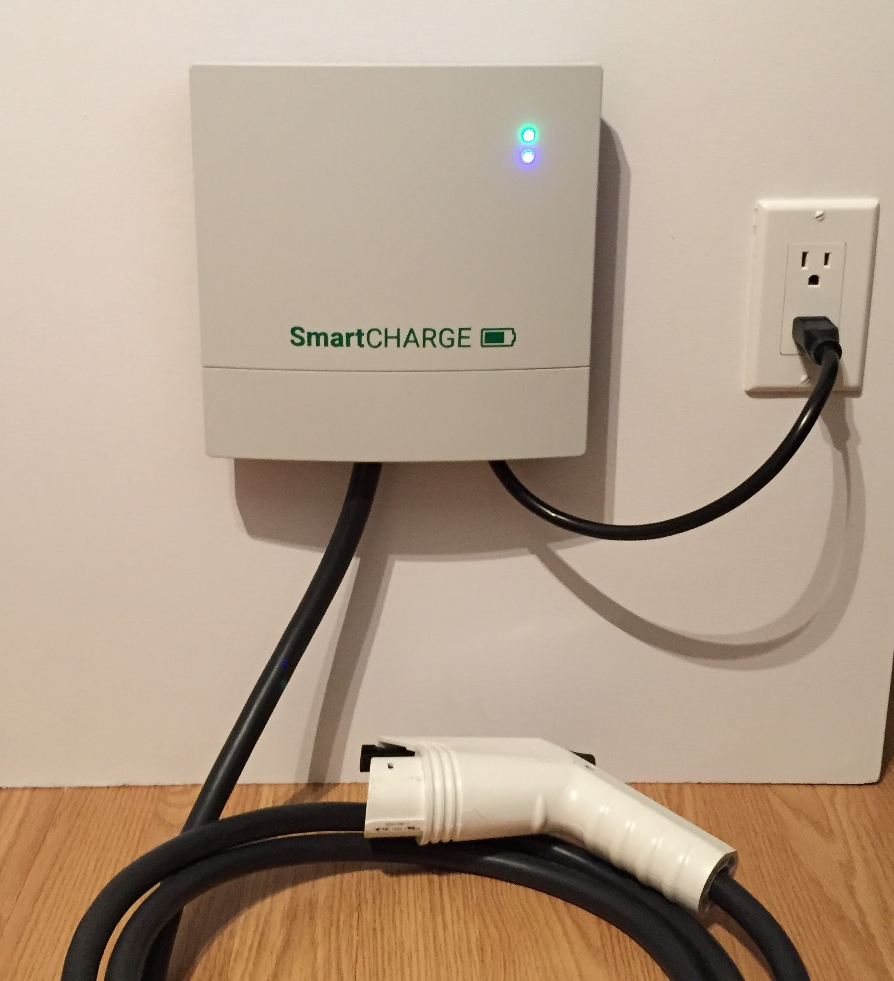
Enclosure design